The Objective of this project was to design and build a PCB which was capable to actuating an electromagnet to produce a range of magnet fields in either direction. This PCB would then be used in the Umbilical of a rocket for the Yellow Jacket Space Program.
Choosing a Design
The first step was to decide how to implement this PCB. I needed a design which could alter the current to the electromagnet, and change the direction of the current as well as stop the current flow completely.
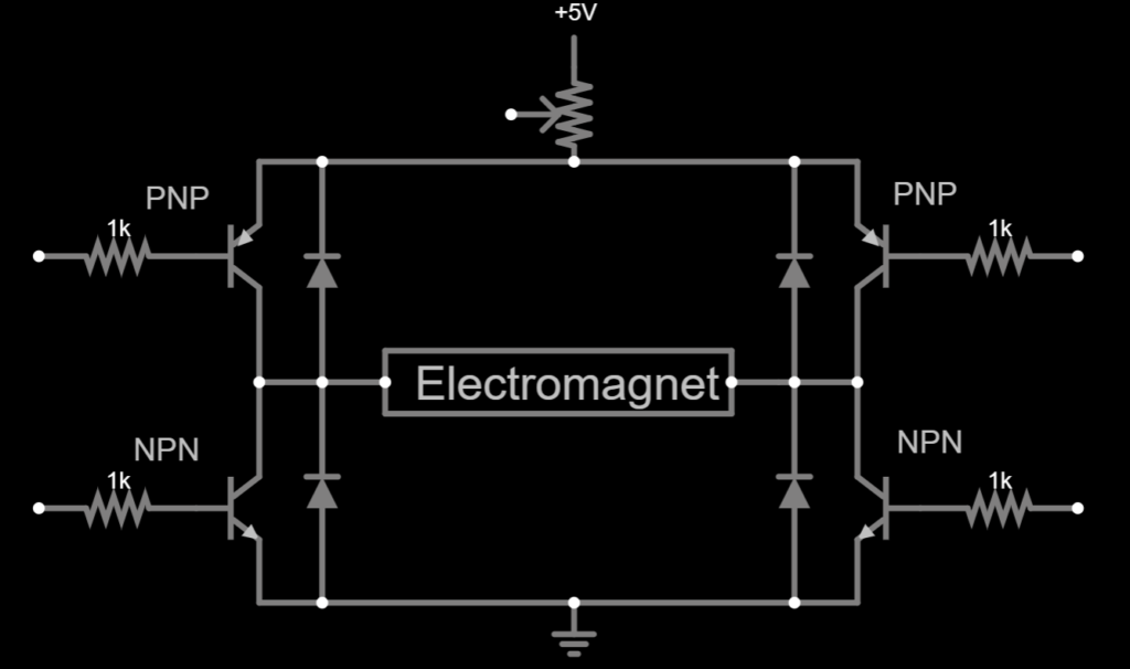
After about a week of research, I stumbled upon the full bridge topology, often used to control motors, and realized it would accomplish everything I needed for this PCB. To implement the full bridge, my initial thought was using P-channel and N-channel MOSFETS with one gate drive and an invertor. However, a little more research revealed that the lag on the P-channel MOSFETS would be too significant to make them practical. Hence, I later altered my design to include only N-channel MOSFETS and use two gate drivers instead of one.


Choosing the Parts and Drawing a Schematic
The next step was to pick my parts and draw the schematic. This step undoubtedly took the longest, but was also the most educational.
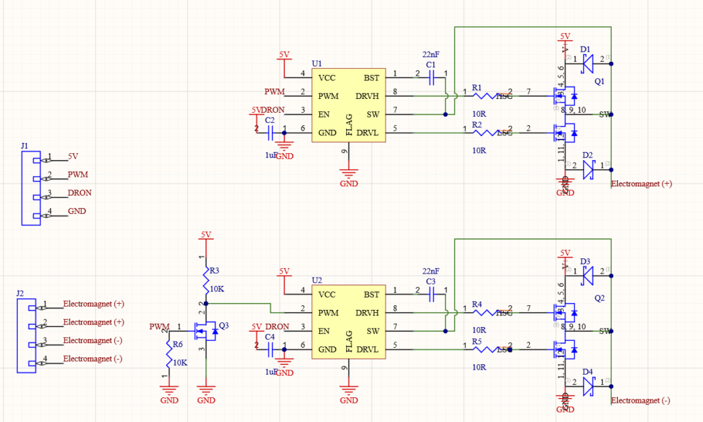
Initially, I was a little lost on how to begin. I started by choosing an electromagnet and looking at the voltage and current ratings. Then, went backwards and picked MOSFETS capable of channeling the necessary voltage and current; I found dual N-channel MOSFETS such that I would only need one chip for each side of the full bridge. Next on the list was picking a gate driver, and upon choosing a suitable one, I made my own invertor using a couple resistors and another N-channel MOSFET.
A key change I made during this step was to use PWM input to vary the current to the electromagnet rather than a potentiometer like I had initially planned. Prior to this project, I had only heard the term PWM and had little knowledge of its applications. However, upon taking a deeper dive into it at the suggestion of one of my teammates, I realized this would be ideal to vary the current to the electromagnet and found a gate driver which could use the PWM signal to increase the impedance of the MOSFETS rather than directly alter the source voltage.
Designing the PCB
With the Schematic made and the parts chosen, the last step was to design the PCB. This too was a extremely educational to me, although thankfully not as research heavy and time consuming as creating the schematic.
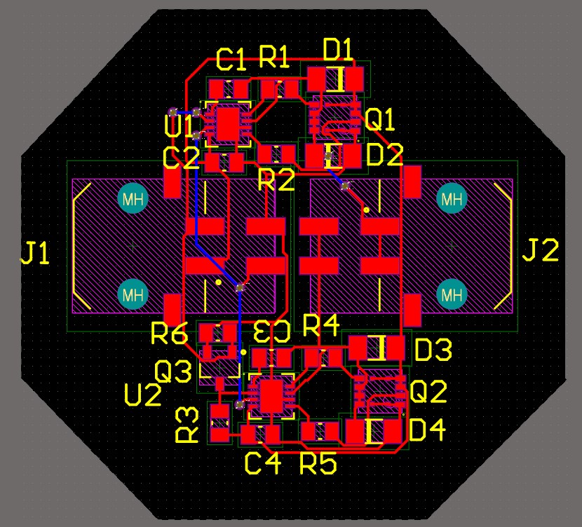
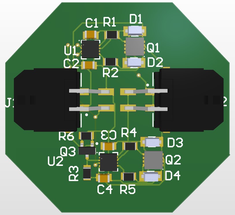
My first step was to lay the parts on the board in the most compact way one side at a time. Then, route the connections between the parts. Although seemingly trivial, I found this process to be very mentally stimulating because laying the track in the most compact way required a surprising amount of critical thinking. Using Altium for this purpose also proved to be a steeper learning curve than for drawing the schematic: many hours were spent looking for tutorials on how to do things such add a second layer to the board or define the board shape, but I enjoyed the learning and am proud to have acquired this knowledge.


Last Step: Building the PCB
My final step for this project is to build the actual PCB and test it. Unfortunately, I am still waiting for my parts to arrive, but I look forward to receiving them and am excited to see the end result. To prepare for this step, I attended a training on PCB design provided by YJSP. Included in the training was hands-on experience soldering a basic PCB with a resin board, an integrated circuit, and a few LEDs, resistors, and capacitors. I look forward to applying the skills I learned in the training to the assembly of my PCB in the coming weeks.